MoS2: The tiny material with big potential
Imagine a material that is only two atoms thick, yet has the potential to revolutionize the way we interact with light. This is the world of MoS2, a tiny yet mighty material that has been making waves in the scientific community due to its unique properties. In this blog post, we’ll delve into the fascinating world of MoS2, exploring its electronic properties and the exciting possibilities it holds for developing advanced sensors and optoelectronic devices.
What is MoS2?
MoS2 is a type of transition metal dichalcogenide (TMD), a class of materials that are composed of two elements: a transition metal (such as molybdenum, tungsten, or titanium) and a chalcogen (such as sulfur, selenium, or tellurium). MoS2, in particular, is made up of molybdenum and sulfur, and is found in nature as a mineral called molybdenite.
MoS2 is unique because of its two-dimensional (2D) structure, meaning that it is only a few atoms thick. This property makes it an ideal material for a wide range of applications, from electronics to energy storage. But what makes MoS2 truly special is its ability to respond to light in a way that is unlike most other materials.
Persistent Photoconductivity: A Unique Property
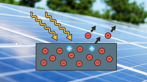
When MoS2 is exposed to light, it exhibits a phenomenon known as persistent photoconductivity (PPC). PPC is a property that allows MoS2 to retain its electrical conductivity even after the light source is removed. This is because electrons become trapped in defects within the material, influencing its electronic behavior.
Researchers have long been fascinated by PPC, as it has the potential to revolutionize the way we design and build electronic devices. In a recent study published in the journal Nature Communications, a team of scientists from the Indian Institute of Technology (IIT) Delhi explored the effects of defects on MoS2’s electronic properties.
The Role of Defects
The researchers discovered that defects in MoS2 play a crucial role in PPC. These defects are essentially imperfections in the material’s crystal structure, which can be caused by a variety of factors, including contamination, radiation damage, or thermal stress.
When a defect is present in MoS2, it can trap electrons, altering the material’s electronic behavior. This is known as a trap state. The trapped electrons can then influence the material’s response to light, causing it to exhibit PPC.
Implications for Advanced Sensors and Optoelectronic Devices
The discovery of PPC in MoS2 has significant implications for the development of advanced sensors and optoelectronic devices. For example, MoS2-based sensors could be used to detect changes in temperature, pressure, or chemical composition, making them ideal for a wide range of applications, from medical diagnostics to environmental monitoring.
Optoelectronic devices, such as solar cells and light-emitting diodes, could also benefit from MoS2’s PPC properties. By harnessing the power of light, these devices could be designed to operate more efficiently and with greater precision.
Conclusion
MoS2 is a tiny material with big potential. Its unique properties, including PPC, make it an ideal candidate for a wide range of applications, from electronics to energy storage. As researchers continue to explore the properties of MoS2, we can expect to see the development of new and innovative technologies that will shape the future of our world.
News Source: